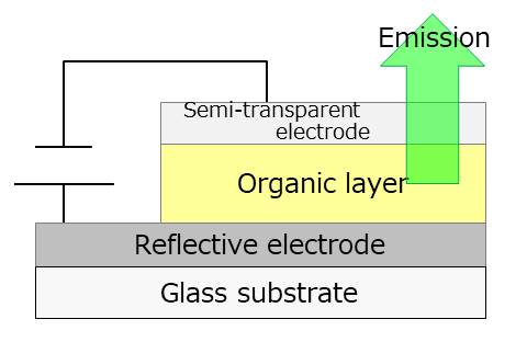
Top Emission Devices
A top emission architecture out-couples the light to the direction opposite to the backplane and therefore, secures a high aperture ratio. With the top emission concept, a micro cavity effect is available by choosing optimal thin-film thicknesses, leading to a high color saturation.
The top emission architecture, however, requires high-quality skills in OLED fabrication, including the skills in preparation of the substrates and in control of the deposition thicknesses.
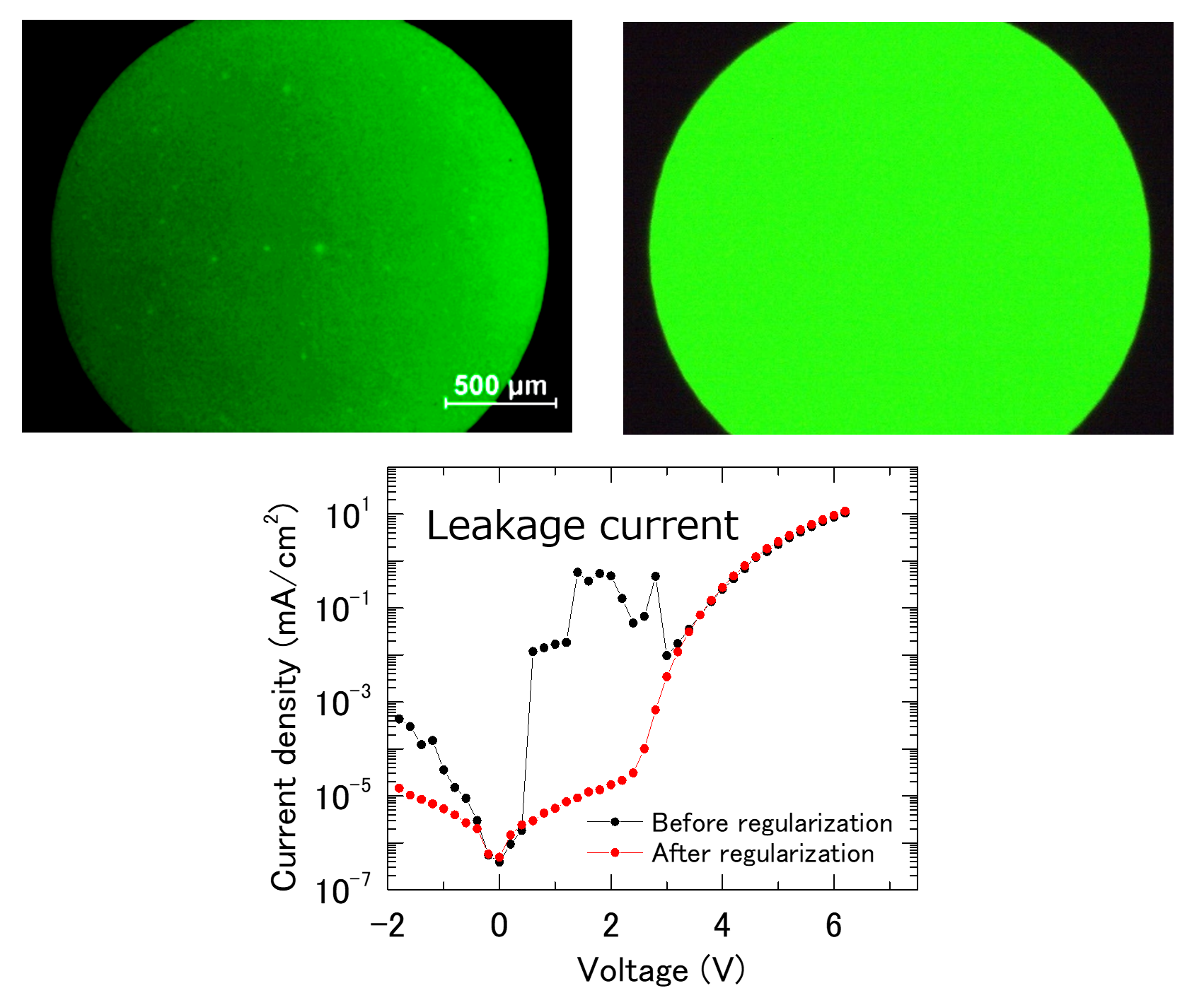
Development of Substrate Cleaning Process
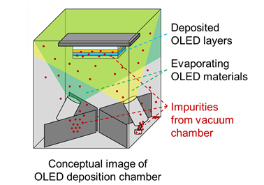
A top emission substrate composes of a reactive metal such as an Ag-alloy. An increasing surface roughness of the substrate is a critical process issue, which is due to oxidation during the storage and the wet-cleaning. We have developed an optimal cleaning process to restrain the occurrence of defects such as white spots and/or leakage currents.
Left figure:Before development、Right figure:After development
Optimization of Top Emission Architecture
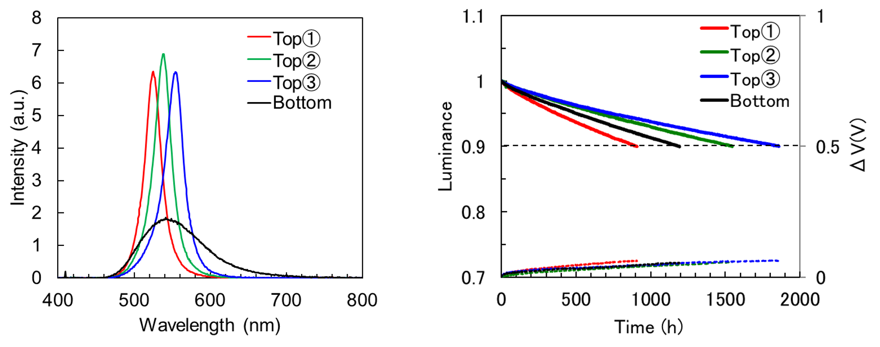
By optimization of a top emission architecture, narrower FWHM and higher absolute intensities of the emission peaks are obtained in comparison to a bottom emission one. The optimized devices exhibit nearly identical or even superior lifetimes to the bottom emission reference.